The concept of Chiclet has exploded, and the company's stock price eight consecutive daily limit | Focus analysis
Author:36 氪 Time:2022.08.17

When the creation core becomes Pindu Gao.

Wen | Zheng Cancheng
Edit | Peng Xiaoqiu
Source | 36 氪 South China (ID: south_36kr)
Cover Source | Pexels
The stock price rose from 9 yuan to 20 yuan, which only took more than a week. This is the charm of Chiclet concept.
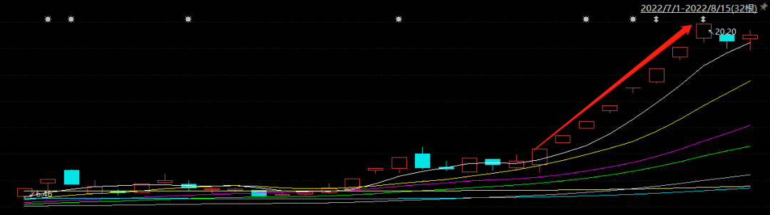
(Dagang Co., Ltd. 8 consecutive daily limit, data source: Oriental Fortune)
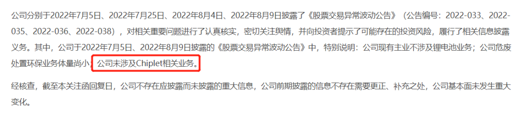
However, the company (Dagang Co., Ltd., 002077.SZ) said in a reply to the Shenzhen Stock Exchange that he did not involve Chiclet -related businesses.
(Daigang Co., Ltd. Corporation, Source: Oriental Fortune)
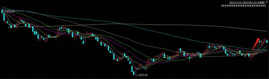
As the new market main line, Chicet has also contributed a new driving force for the semiconductor index. The entire index rose by more than 17%from August 1st to August 8th. IP authorization is also a subdivision segment that benefits the Chiclet. The head -of -headed company core original shares (688521.SH) also rose from 44 yuan to 72 yuan, an increase of 63%.
(Semiconductor index (801081.swi) trend chart, data source: Oriental Fortune)
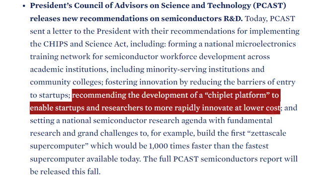
What is CHIPLET? This concept was first mentioned by the founder of the MARVL.O (MRVL.O) in 2015, but it was mentioned in the recently signed "2022 Chip and Science Act". That is, the Presidential Science and Technology Advisory Committee (PCAST) began to "propose to establish a Chiclet platform."
(Classification of the bill, Tuyuan Network)

The key of the Moore era
Chiclet is translated as "core grain", and its core idea is Lego's modularization -the several small chips are assembled into large chips by packaging technology to achieve performance improvement and cost reduction.
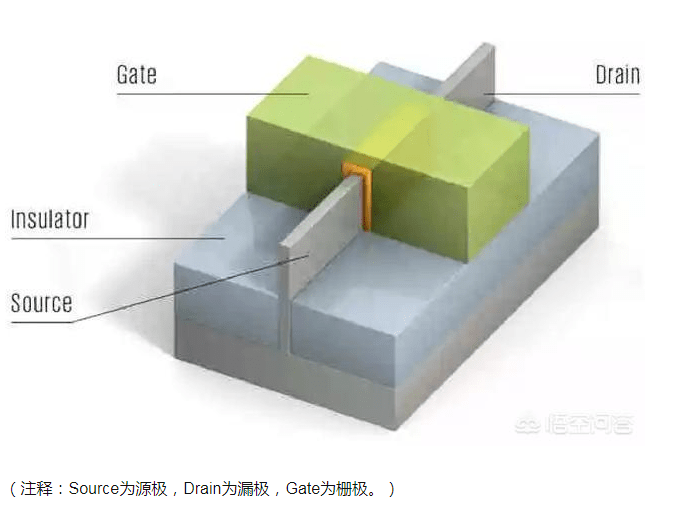
Before knowing Chiclet, we must be familiar with several concepts of the semiconductor industry. One is Moore's Law that has always followed the development of integrated circuits. "Every 18-24 months, the number of transistors in the chip doubled." The law proposed by Intel was Gorden Moore, the founder of Intel, and in 1965 he also worked at Sendong Semiconductor Corporation.
The other is the transistor. As the main component of the chip, the number of transistors directly affects chip performance. Therefore, since the chip was invented, scientists have tried their best to stuff more transistors under a certain area. In simple terms, as shown in the green part below, the smaller the width, the more the crystal tube can be plugged in the unit area, the higher the performance of the chip.
(Drama diagram, picture source network)
This width is also called process or technical node. After the continuous breakthrough of the technical node through the wafer factory, although the battlefield of TSMC and Samsung in the head chip manufacturer has reached 3nm, the interval between the breakthroughs of adjacent technical nodes is getting longer and longer Essence
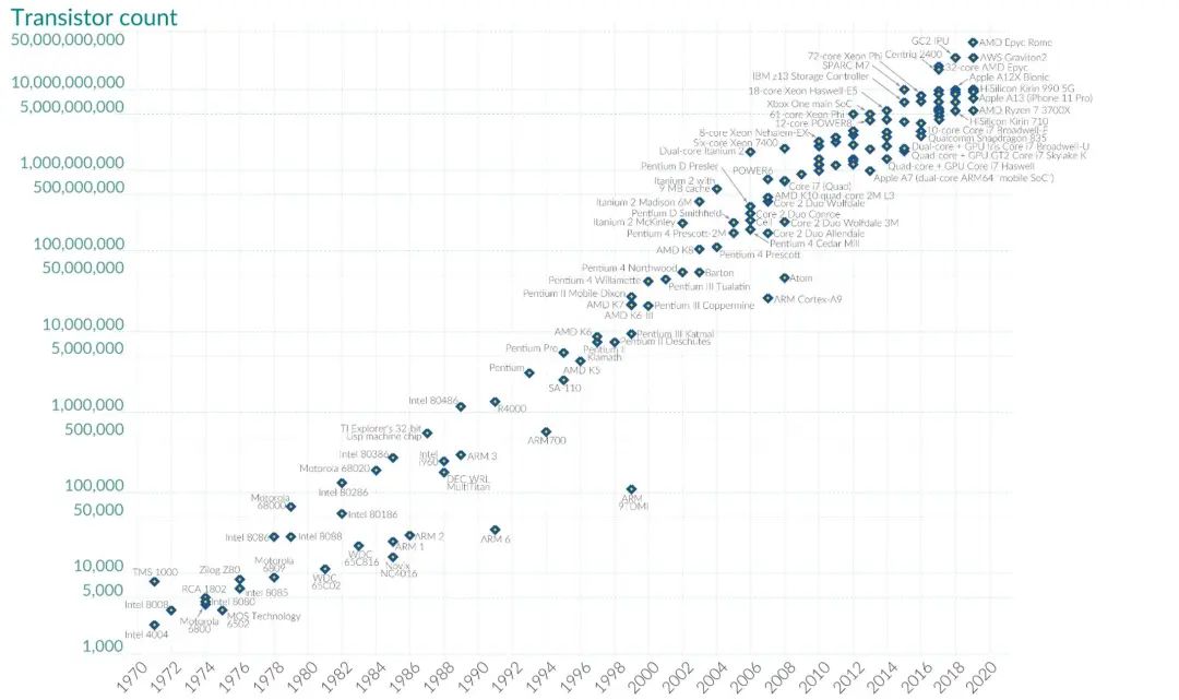
(Search chart of the crystal tube, data source: wikipedia, Minsheng Securities Research Institute)
In addition, in this breakthrough process, the research and development of each process requires a huge amount of capital investment, and the breakthrough of nodes is not proportional to the capital investment. 36 氪 learned that the R & D investment of the 5nm process is almost the sum of 7nm and 10nm investment. This has led to the on the way to breaking the new node in the fabry factory, and some players will choose to give up halfway. For example, Lianhua Electronics (UMC.N) announced in August 2018 that it had abandoned the development of advanced technology below 12nm; shortly after, Giro Fangde announced the abandonment of 7nm research and development.
However, the downstream applications not only did not slow down the pursuit of chip performance, but also put forward higher requirements for the "occupied area" of the chip. For example, the equipment such as TWS headphones, AR and VR is small, so the performance of several chips can be concentrated on one SOC (System On Chip, System) chip.
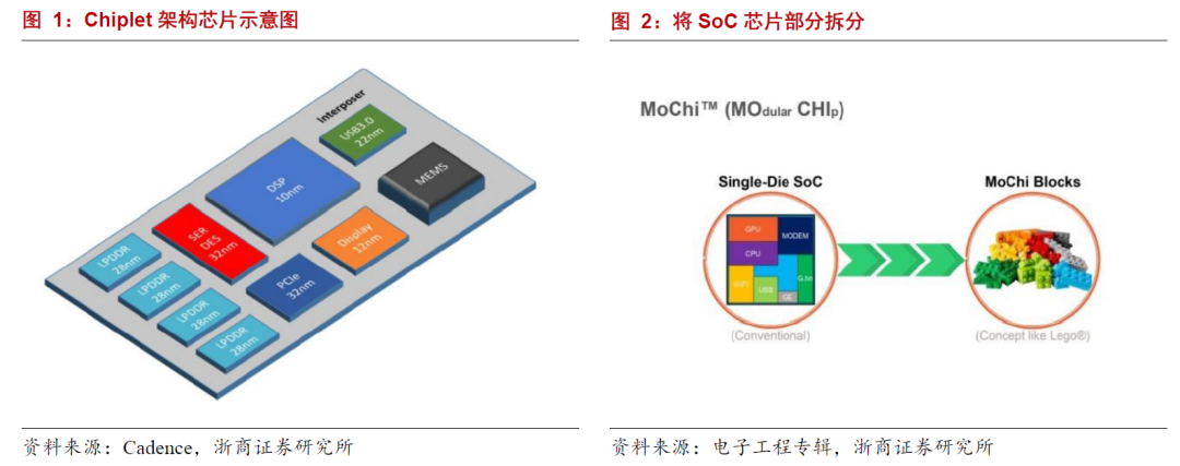
Note: The name of the MOCHI is the name when the first proposed by Chiplet
Chiclet uses the dimension of "height" to disassemble the chip that was originally on a plane, and then assembled it like a blocks. This can not only save the area, but also make each small chip have more space, but also bring higher economic benefits.
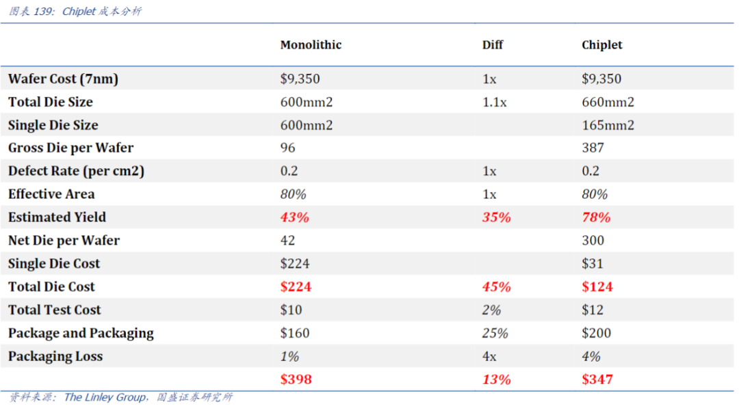
First of all, Chiclet can flow separately (trial production) alone to reduce the risk of the failure of the stream. With the continuous improvement of technical nodes, more and more IPs (functional modules of large chips) integrated by single chips will be increasing. According to IBS data, the number of IP integrated 7nm and 5nm process integration is 178 and 218, respectively. When a streaming film, any IP error will lead to a failure of the flow, which will cause a certain impact on the chip design company's cash flow. For example, the 7nm craft chip is cost 30 million yuan at a time, and 5nm is more than 47 million.
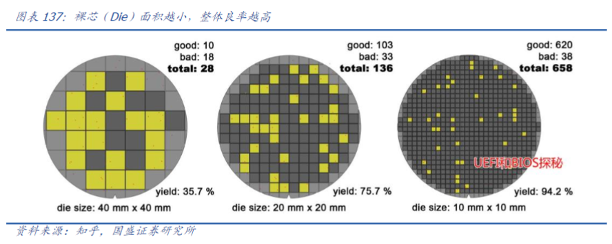
Secondly, Chiclet can improve the yield of manufacturing. "The chip is made of sand, but the chip cannot tolerate 'a grain of sand'", and an industry insider told 36 氪. In fact, the chip is produced in a high dust -free environment, and its cleanliness of the environment is higher than the operating room. This is because as long as a dust falls to the chip, the chip may fail.
The fall of dust is often random and completely unpredictable. In other words, the greater the chip, the greater the possibility of staining dust, and the lower the overall yield. Guosheng Securities data shows that when the overall area of the chip is 10mm x 10mm, the yield is 94.2%; but if the area increases to 16 times, that is, the 40mm x 40mm is only 35.7%. Note: DIE in the figure indicates nude films, that is, the state before chip packaging
Finally, Chiclet can improve reliability. Due to the limitation of the chip manufacturing end, a chip can only use the same technical node. For SOC chips that integrate multiple functions, higher technical nodes will reduce reliability. For example, IP -related IPs are suitable for using more mature craftsmanship and lower technical nodes. Pursuing small line width may occur, leakage and noise.
The above advantages make Chiclet more cost -effective than continuing to break through the advanced process. The consulting company The Linley Group estimates that under the 7nm process, Chiclet saves nearly 13%compared to the traditional single -chip solution.
In addition, it should be noted that Chiclet is not better than traditional solutions in each item. In the test and packaging link, a large chip is divided into several small chips instead increase work difficulty and workload. According to GROUP, the cost of 2%and 25%is required in the two links of the 7nm process.
The rest, hand over to the packaging

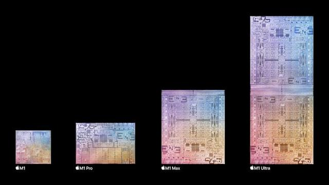
Although Chiplet technology is not yet mature, some pyramid players have started early exploration. For example, the M1 Ultra chip released by Apple is based on the M1 MAX, using Apple's bridge technology to connect the two 5nm process M1 MAX chips together.
(Apple M1 Max M1 Ultra, Tuyuan Network)
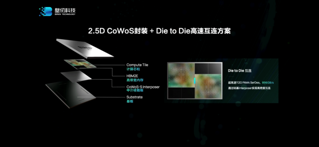
Recently, the GPU chip BR100 and BR104 released by the wall of the wall also adopted the above solution. At the press conference, Hongzhou, co -founder and CTO, co -founder and CTO of Wall -创 Technology, said, "The BR104 released by Gradma Technology is a single DIE (nude) product, and the BR100 is a dual DIE product using Chiplet technology. Formed two products, each has its own advantages and focus, covering a broader application market. "
(BR100 uses Chiclet technology, Tuyuan Network)
It is worth noting that the wall -sized technology products and Apple products use different packaging technologies to "stitch" two chips together. In addition, internationally renowned chip companies such as AMD and Intel have also begun to deploy Chiclet, but they are only limited to their own products. Different chips that different chip companies are not compatible.
Similar to the relationship between the mobile phone charging port and the charging cable, even if there is a Type-C now, there is room for compatibility between the charging equipment. Besides, before Type-C, the charging port was even more diverse. Small chips that form a chip system also have many interface standards now, such as the Gen Z alliance where AMD and ARM and other companies are located; the CXL alliance where Intel, Cisco and other companies are located.
Now, the uniform chip standard similar to the Type-C status has been in progress. In Q1 in 2022, the semiconductor industry head company formed the Chiclet standard alliance, UCLE (Universal Chiclet Interconnect Express), which defines the Chiclet connection standard, the purpose is to form a chip interconnect ecology. With this ecology, some mature IPs can be used by chip design companies to reduce the cost of chip design and reduce the research and development time.
In fact, in addition to the interface standards, Chiclet has three major problems that need to be solved.
First, Chiclet has a higher calories under the same crystal density. This is because the interconnection between the chip and the chip is always not as direct as the crystal tube. Although more transistors are plugged in the same area, the power consumption has become the next issue that needs to be balanced; second, the relevant EDA software has not yet been launched;
Third, Chiclet is not a simple fight. The connection between the chip and the chip needs to be drilled with two naked pieces, and then the circuit is connected through the precision electroplating method. For example, the drilling link, the thickness of the wafer is only about 100 microns (1 meter = 10^6 microns). Under such thickness, drilling requires micron level accuracy control. If the wafer is not well controlled, the wafer will be penetrated.
Even in the face of many challenges, Chiclet is still the trend of the development of the Moore era chip development.
36 氪 Public account

I sincerely recommend you to follow

= pngwx_head = 1 "data-nickname =" 36 氪 South China "data-alias =" south_36kr "data-signature =" 36 氪 under the official account. Focus on the Greater Bay Area, radiate South China, with business connecting the world, forward-looking, depth, letting let the world look forward to the world.Some people go to the future first! "Data-from =" 2 "data-is_biz_ban =" 0 "has-int-parting =" 1 "data-index =" 0 "data-Origin_num =" 374 "data-isban ="0 " /> Come" Share, like, watch "
- END -
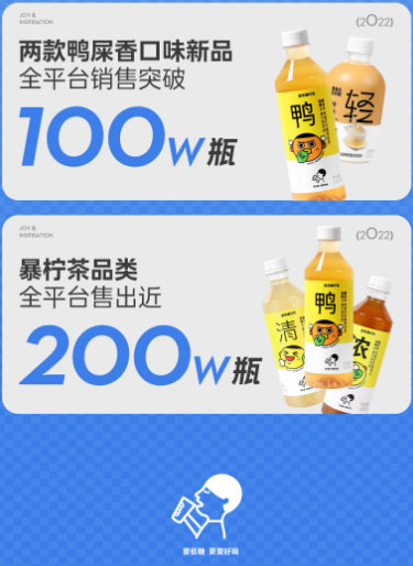
Several new consumption | View new consumption through "618": bottled lemon tea demand surged, prefabricated vegetable search skyrocketed 877% | Cover every day
Cover reporter Ouyang Hongyu Wu YujiaWith the end of the 19th 618 promotion season...
The surplus of the economic forest has become a treasure on the spot
In the cultivation of the tea seedlings, after we changed to a new formula develop...