Progress | Ultra -high vacuum mechanical stripping and stacking technology made progress
Author:Institute of Physics of the Ch Time:2022.06.16
In recent years, the two -dimensional materials and his heterogeneous structure have received widespread attention from people in the fields of electronics, photoelectric and spinning devices. However, the two -dimensional materials that are highly clean on the surface and the flat and clean two -dimensional heterogeneous knot of the interface atomic level are still very difficult, especially for the surface -sensitive two -dimensional materials. The method of preparing two -dimensional materials is mainly divided into two categories: the "bottom -up" method represented by molecular beam extension (MBE) and chemical gas deposition, and the "top -down" method represented by mechanical divestituting. Among them, because the "from the bottom up" method is restricted by growth dynamics, it can only prepare specific two -dimensional materials on a specific background, and the prepared two -dimensional materials usually have a certain orientation. Therefore, it is greatly limited to it. Types of the two -dimensional alien knot obtained. Compared with the "bottom -up" material synthesis strategy, the "top -down" method represented by mechanical stripping has the characteristics of simple operation and strong flexibility. Traditional growth methods are difficult to achieve, small -layer samples and corner structures. However, the traditional mechanical stripping method is carried out in the atmosphere or glove box, and there are still many problems: (1) the pollution of the environment will introduce a large amount of impurities or defects. Even for the stable two -dimensional materials (such as graphene), the sample prepared by this method, such as without annealing, is passed into the vacuum, because the surface is adsorbed on the surface, it is difficult to use surface -sensitive technologies such as ARPES, STM, etc. Measurement, and high temperature annealing may introduce more impurities or defects. (2) Many single crystal surfaces cannot exist in the air or even low vacuum environments, such as SI (111) -7 × 7, CU (111), Fe (100), etc. The surface of these materials will inevitably be oxidized and adsorbed A large amount of impurities. Therefore, the traditional mechanical divestation method cannot prepare the heterogeneous interface of two -dimensional materials and such substrates.
Recent Wait, the independent design and setting up a set of two-dimensional material mechanical stripping system in a high vacuum environment. They combine mechanical stripping technology with ultra-high vacuum MBE technology. In the environment of the 10-10MBAR magnitude of the base, MBE technology has been used to prepare a variety of atomic levels of flat and clean surfaces, and using mechanical stripping technology on these. A variety of single -layer and small -layer two -dimensional materials were successfully stripped on the substrate.
The working schematic diagram of the device is shown in 1, and all operations are completed in ultra -high vacuum. First of all, they used a variety of surface treatment technologies such as high temperature annealing, ion sputtering, plasma etching, and MBE growth to obtain the flat and clean surface of the atomic level. The quality of the surface can be confirmed through an ultra -high vacuum surface analysis method such as scanning tunnel microscopes, low -energy electron diffraction, and angular optical electronic energy spectrum. Then, they explained the two -dimensional material in the ultra -high vacuum, obtained fresh surfaces, and gently pressed it on the surface of the substrate. Finally, they heated and separated the system and obtained a variety of single -layer and small -layer two -dimensional materials. Using this method, not only did they repeat the golden auxiliary peeling technology under the atmosphere, but also successfully obtained a variety of two-dimensional heterogeneous knots that have not been reported before, including BI-2212/Al₂o ₃, BI-2212/SI (111), MOS₂ /Si (111), MOS₂/Fe, MOS₂/CR, and Fese/SRTIO₃ (any angle), etc.
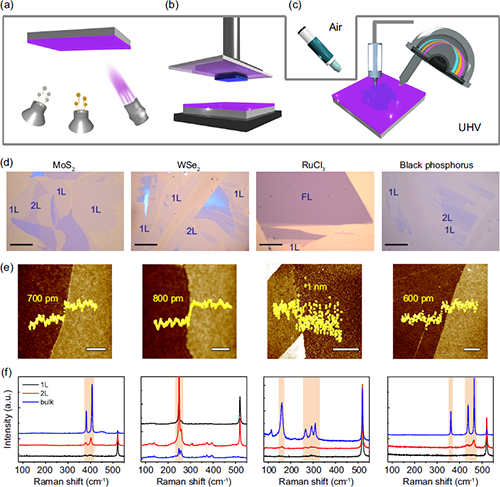
Figure 1 Ultra -high vacuum mechanical stripping two -dimensional materials
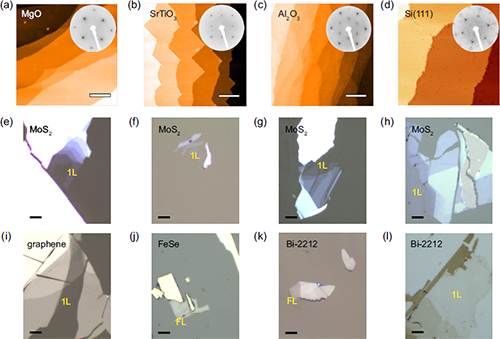
Figure 2 Ultra -thin two -dimensional materials obtained on a single crystal substrate
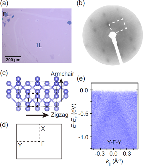
In order to further display the ability of the system, they chose two systems as an example. (1) Using the gold -assisted divestiture technology, they prepared millimeter -level single -layer black phosphorus samples in ultra -high vacuum, and used the low -energy electron diffraction and angular optical electronics spectrum of the original position to represent the samples. The diffraction spots and the cavity type in the direction of the high symmetrical direction (Figure 3). This is the first international measurement of single -layer black phosphorus. (2) In order to reveal the impact of different metal substrates on the material nature of QR, they studied the optical properties of single -layer MOS₂ and WSE₂ on different metal surfaces (Figure 4). By measuring the fluorescent spectrum of single -layer WSE₂ on different metals, they unexpectedly discovered that except for AU substrates, the remaining AG, Fe, CR and other surfaces are not quenched to destroy the features of WSE₂ Shoot. Through the Raman spectrum, they found that MOS₂ on the surface of AU and AG, its characteristic Raman Peak E₂g and A₁G except for frequency movement, showing strange split behaviors.
Fig
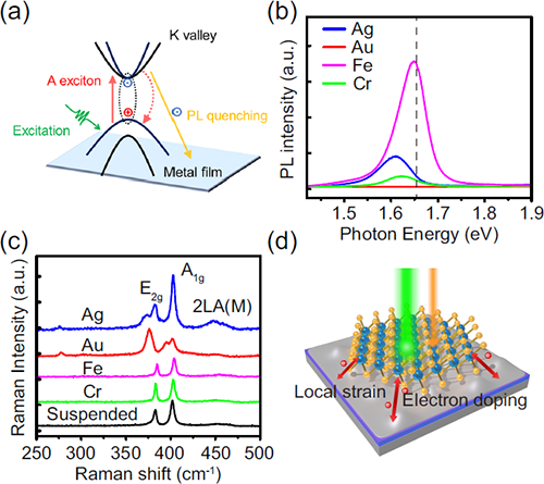
Figure 4 The optical response of different metal surface single layers of WSE₂ and MOS₂
This work provides a new method for further preparing high -quality two -dimensional materials and heterogeneous samples, the nature of the research materials, and the interface acting phenomenon.The related results were published on Science Bulletin (Doi.org/10.1016/j.202222.05.017) in the "Exfolship of 2D Van Der Waals In Ultrahigh Vacuum for Interface Engineering".The work has been funded by the National Natural Science Foundation of China, the Ministry of Science and Technology, the Beijing Natural Science Foundation of China, the International Cooperation Project of the Chinese Academy of Sciences, and the leading project of the Chinese Academy of Sciences.Edit: Just_iu
- END -
The 192 mobile phone number is here!Shandong Cheng's first batch of 20 provinces to launch 5G network services in the country
Popular Network · Poster Journalist Lu Le Correspondent 逯 Jiaqi Jinan ReportOn J...
Famous teachers 2 2022 Issue 3 "Deep Learning Security and confrontation" special responsibility editorial board recommendation paper
Deep Learning Security and confrontation is the third topic of Information Securit...