From electricity to light, the Chinese chip industry is moving towards the light | Jiazi Guangnian
Author:Jiazi Guangnian Time:2022.08.25
The Chinese core opportunity in the Moore era
Author | Xiaoxian
Edit | chestnut
After the law of Moore's law fails, traditional battery chips gradually approach the performance limit, and more and more practitioners turn their attention to light.
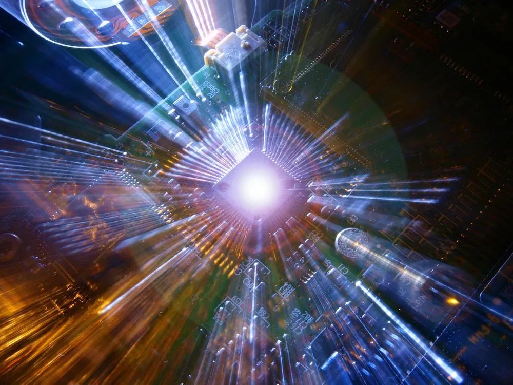
Compared with electronic chips, the characteristics of light chips are at high speed and low power consumption. In the field of communication, optical fiber communication supports 5G coverage in data transmission, and the calculation and storage field also leaves a huge stage for optical chips.
The performance potential of the light chip far exceeds the power chip has made it a determined track for the development of hard technology. In recent years, overseas chip manufacturers such as Intel, Nvidia, Gexin, etc. have shot and purchased the optical chip project, and the layout of the new track has been arranged. In China, Huawei and other manufacturers have also invested more than ten optical chip companies to cover upstream and downstream of the industrial chain.
From the perspective of technological competition, optical chips are considered to be chip technology with the smallest gap with foreign research progress, and they have attracted the hope of "overtaking" in China.
Professor of the School of Information Science and Technology of Peking University, He Jin, director of the key laboratory of Shenzhen System Chip Design of Peking University, said to Jia Ziguang that it was the focus of the development of the chip industry from the battery chip to the optical chip. Relying on a huge application terminal, China may be done with foreign countries in the future.
From electricity to light, the Chinese chip industry is moving towards the light.
1. The dawn of the Moore era
The crystal density develops at a speed of double the speed every 18 to 20 months. The performance of the battery chip is doubled every two years, and the price drops to half the previous. Over the past 50 years, the computing power of the chip has been following Moore's law.
But now, the calculation chip has begun to develop from 5 nanometers to 3 nanometers, and the diameter of the atom is about 0.3 nanometers. After the process of 3 nanometers, the limit of physical, technical and cost will approach infinitely.
Although the growth of computing power slows down with the limit. But with the continuous popularization of digitalization and intelligence, human society's demand for computing power is still expanding sharply.
According to the statistics of American Artificial Intelligence Research Company, since 2012, the computing power demand for artificial intelligence has increased by an average of double the average of 3 to 4 months. Today, the largest neural network model is 15 to 300,000 times 10 years ago.
The computing power of the battery chip is caused by multiple reasons. For example, when the size of the chip is less than 5nm, it may bring the "quantum tunnel penetration effect". Moreover, even if the transistor is smaller, the power consumption during the operation of a single transistor is difficult to reduce, and the heat generated cannot be effectively dispersed. This physical characteristics directly determine the calculation density that can be done on the unit area of the electrical chip, and it is difficult to have room for improvement.
In addition to making the transistor smaller, expanding the area of the battery chip is also a way to enhance computing power in the industry in the past. But this approach will also face the problem of power consumption. The increase in the area of the chip means that it requires a longer wire, and the chip electrical energy consumption is proportional to the length of the wiring. The wire power consumption is too high, which is undoubtedly the bottleneck that cannot be around the entire system. The end result is that the chip is bigger, and the power consumption will increase significantly with the increase.
The size of the battery chip is about to be reduced to the limit, while expanding the area cannot efficiently improve the computing power. The two roads when the battery chip is seeking breakthroughs in higher computing power is difficult to get through.
At this time, the optical chip was given a high hopes for breakthrough composition.
In fact, for decades, scientists have been committed to finding a way to use light for information transmission processing. This exploration of light is even earlier than electric chips.
In 1960, American scientist Shi Odo Meman invented the world's first visible light output laser, which made major breakthroughs in optical development. This means that humans have entered a new stage of lighting, mastering and utilization of light.
During the same period, Chinese scientist Gao Yan proposed to replace copper wires with glass fibers and replace current with light. After the application of breakthrough technology, this breakthrough technology has developed into a fiber -fiber communication in long -distance communication.
Looking back at the development of the light chip, as early as 1969, the Bell Laboratory in the United States has proposed the concept of integrated optics. However, due to technology and commercialization, it was not until the beginning of the 21st century that companies represented by Intel and IBM began to cooperate intensively to focus on the development of silicon chip optical signal transmission technology.
Since the development of light communication, light has fully proved its advantages in data transmission. At present, all long -distance communication, including the data between the server and the server in the data center, is performed by optical fiber instead of copper wires.
In recent years, people have begun to "transmit" attention from the data of light to "processing". Compared with micro -electron chip electricity signals as information carriers, the optical chip uses a higher frequency light wave as an information carrier.
Compared with integrated circuits, the optical chip has avoided the problem of fever in technology. The transmission loss is lower, the bandwidth is higher, the delay is less, and the anticroxyomomy interference capacity is stronger. These are the huge advantages of optical chips.
"Today, we have discovered the great ability used by photons for information carriers in optical fiber transmission. If photons are transmitted and processing information inside the chip system in the future, it is a moment of excitement. The fastest medium. "He Jin, a professor at the School of Information Science and Technology of Peking University, and the director of the key laboratory of the Shenzhen System Chip Design of Peking University.
At present, silicon light technology has been widely used in the field of transmission, carrying information transmission tasks in the field of large data centers and telecommunications. The field of light sensing represented by laser radar is also gradually maturing. Calculation based on silicon light chips is expected to gradually appear in some computing scenarios in the next 5-10 years. In the context of the Chinese chip industry being stuck in the neck, the light chip has the meaning of another layer of "transforming the road".
The development of the battery chip is a process of accumulation, which means that it is difficult to "make up the operation" in a short period of time. He Jin said: "There is a gap between the 4-5 generations of Chinese battery chips and foreign countries, but the optical chip is still in the research and development stage worldwide, and has not yet been applied to intergenerational differences. Therefore, relying on China's huge huge itself The application terminal and the unique unified market, we may be synchronized with foreign countries in the industrial application of optical chips in the future. "
2. The birth of a light calculation chip
Although the development of light chips has been highly hoped, for a long time, light computing is a technology that has been trapped in laboratories and universities for a long time. In 2017, Shen Yichen, a doctor of physics from MIT, opened a breakthrough in an article about AI computing light chips.
At that time, Shen Yichen published an important academic achievement of integrated photon computing at the position of the cover thesis in the journal "Nature -Photon" journal. Control the interference between these light. When these light interfere with each other and these numbers are calculated, the entire calculation time is the time of the light through the chip: 0.1 -0.5 nano. The same large matrix multiplication is about 100 times the operation time on the battery chip.
This paper has become a major node for the development of photon computing chips. It has caused a huge response in the academic and industry, and investors and entrepreneurs have come to the door. This has also become a major driving force for Shen Yichen to go out of the laboratory and establish a company. In the same year, Shen Yichen founded Xizhi Technology of photon AI chip company. The second author of the paper Nicholas Harris founded LightMatter in the same technology field.
Recalling the scene at that time, Shen Yichen said: "Xi Zhi Technology was one of the earliest companies. When founding, even AI chips were a new concept, let alone photon AI chips. Calculate this cutting -edge technology into one category. "
As the results of industry giants such as Intel and Nvidia gradually released in the field of photon computing chips, the process of running through scientific research to industrial and photon AI chips began to step from being questioned to widespread recognition. The confidence of entrepreneurs and markets is becoming more and more obvious. In 5 years, the global photon AI chip company has increased from one or two from one or two to more than 20 currently.
According to reports, since the establishment of Xi Zhi Technology, the company's total financing has exceeded $ 220 million. With more than ten MIT doctors as the core, there are more than 200 global teams. The office and laboratory are distributed in Boston, Shanghai, Hangzhou, Nanjing and other places.
Lightmatter, established in the same period, also attracted much attention in the United States. Public information shows that after its establishment, it has won the investment of Jingwei United States, GV (formerly Google Capital), Hewlett -Packard, Lockchid Martin, and the US Department of Defense. Dollar.
"Photon chip is undoubtedly one of the hottest directions in the industry." Shen Yichen said.
At the end of 2021, Xi Zhi Technology launched a computing processor PACE based on photon chips, which is also the first computing system in the world to show photonic advantages. It is understood that the structure of the PACE consists of two parts: light chip and battery chip. The battery chip mainly seizes the data of the data and the mixed number of digital molds, while the optical chip calculates the data. Finally, the light and battery chips are composed of stacking of 3D packaging technology.
The PACE photon chip integrates more than 10,000 photonic devices, and the chip is running at a speed of 1GHz. Compared with the current Nvida GPU3080, which can buy a single computing power on the market, running a specific circular neural network algorithm and the time required for PACE It is less than 1%of the time required for GPU.
Shen Yichen said that this contrast is not to prove that PACE can run all neural networks in general, and the speed is 100 times. But PACE's performance illustrates the upper limit and its potential of light computing advantages.
In addition, the advantages of optical chips are not only reflected in the technology itself. In terms of performance, optical chips are also dependent on advanced process technology.
Shen Yichen said that the silicon light chip does not need to have particularly high requirements for the process. For example, the COMS process line with 65 or 45 nanometers can meet the current optical chips and light computing. The improvement of optical chip performance is more technical from other aspects, including the main frequency, the wavelength and the number of different modes.
Strictly speaking, PACE represents an electronic chip deep -combined optoelectronic mixed operation, not pure light computing. "In the foreseeable future, it will be a mixed optoelectronic mixed operation with electronic chips." Shen Yichen said.
In this way, PACE can be completed through a battery chip in interaction with the outside. All instruction set compilers and SDK are carried on the battery chip, which is compatible with the ecology of the existing chip in terms of software. The optical chip part of the processor work in the main task, including linear computing and data network. Shen Yichen said that Xi Zhi is about to launch a more generalized computing product. If the interconnection of light and the calculation of light are added together, for the first generation of products, as long as it can show a 3-5 times computing power advantage, it is enough to be enough Find huge market space in broad applications.
3. In the Silicon Light, China Opportunities
Although the photon integrated circuit is still in the stage of primary development, there is no doubt that this development trend has become inevitable. In December 2021, the Alibaba Barmamu Institute released the top ten scientific and technological trends of 2022, and the photoelectric chip was also among them.
But it should be pointed out that the emergence of optical chips is not to completely subvert and replace electric chips. In fact, photon chips need to be fused with mature electronic chip technology. The use of advanced manufacturing processes and modular technology of electronic chips, combined with photon and electronic advantages of silicon optical technology will be the mainstream form in the future.
At present, the reasons for immature silicon light are many aspects. The commercialization of chips depends on a very long industrial chain. From design, manufacturing to post -delivery samples and commercial use, the time cycle is counted for several years. At present, the process of silicon light integration has not yet matured, bringing low chip yields, not obvious cost advantages, and non -automated design, design and process disconnection, etc. The upstream and downstream of the industrial chain needs to participate together to form a more complete silicon light ecology.
"Commercialization itself is a continuous and long process. It took 10 years like the popularity of the first smartphone. The computing chip with a mixed photoelectric mixed can be sent to the customer in the next one or two years. The general computing product needs time. "Shen Yichen said.
Generally speaking, the current silicon optical chip industry chain is far less mature as the battery chip. Under the pouring of the chip giant resources, the industrial chain is growing rapidly. The rapid development of lidar, including optical computing and light sensing routes, is driving the increasingly mature silicon light supply chain.
"Especially in the past two or three years, many large wafer factories, EDA design companies, and sealing and testing plants have officially deployed the direction of silicon light." Shen Yichen said. Xi Zhi Technology is also establishing strategic cooperation with front -line wafers and packaging plants to promote the development of silicon light ecology.
Mi Lei, founding partner of China Science and Technology Chuangxing, told Jia Ziguang that "When the foundation was established in 2013, the photoelectric chip was a very unpopular track in China. Working, there are few investment institutions asking. "
Coincidentally, that year, the import scale of Chinese chips exceeded oil for the first time. After capturing this phenomenon, Mi Lei judged that China's chip industry in the future is likely to be "stuck neck". So Mi Lei, who was born in optical background, began to find optoelectronic chip projects in China.
In order to build the photon industry ecosystem, in 2015, China Science and Technology Creative Star launched the first photoelectric chip industry incubation platform -Shaanxi Optical Electronics Pilot Institute, and invested hundreds of millions of yuan to purchase professional equipment, build a clean plant, recruit professional talents, provide provides providing professional talents. Complete supporting services help early chip companies flow.
The following year, China Science and Technology Chuangxing set up an early fund of 1 billion yuan to invest in the field of optoelectronics. In this year, the market environment has turned, and the integrated circuit that has been swept for nearly 60 years has encountered a bottleneck in development. Giant Intel announced that it will no longer launch chips in accordance with the "Moore Law". Mi Lei proposed the "Mi 70" law, calling on everyone to pay attention to the integrated light path.
He believes that future optical costs account for at least 70%in product assembly costs. At that time, optical devices, mechanical devices, and electronic devices may gradually be chipped, or even integrated into a chip.
Today, among more than 370 hard technology companies invested by China Science and Technology Innovation Investment, more than 150 light+semiconductor projects have been promoted to promote the investment layout with the "optoelectronic chip" as the core.
At the recent Emtech China Global Emerging Science and Technology Summit, Mi Lei said in sharing that the scientific and technological revolution in the past 60 years is an informatization revolution driven by integrated circuits and optical communication. A new round of scientific and technological revolution represented by life sciences.
With the maturity of the technical fields in recent years and the implementation of landing applications, the development of the photoelectric industry has continued to speed up.
In 2017, the iPhone X was equipped with a 3D camera. Face recognition technology hidden behind Liu Haiping was widely accepted in the mobile phone field. The VCSEL laser chip as the core component of 3D sensing technology ushered in a well -spraying growth. In the field of autonomous driving, laser radar is an important part of perception. Laser radar represented by Quanergy quickly becomes unicorn in the autonomous driving boom, and also brings more attention to the optical chip.
Huaxi Securities stated in a silicon optical industry report that in 2019, the global silicon light market size was US $ 480 million, and it is expected to grow to US $ 3.9 billion by 2025, a compound increase of 40%.
“总的来说,电芯片时代是用原创技术去找市场,光芯片则是市场爆发需求,反过来研发原创技术来满足需求,从这个角度来说,智能时代,我们有新的业态,新In the need, more people are willing to embrace new technologies than any country around the world. "He Jin said. He believes that at the level of information infrastructure and the level of new IT technology construction, China has greater market demand and more enthusiasm for embracing the new technology ecology. It is better to apply ecology than foreign countries. The advantage has formed a certain advantage in the field of optical chips.
"In the future, China's biggest opportunity must be in the era of light." Mi Lei said in an interview that the infrastructure in the era of artificial intelligence alone, whether it is a 5G network or the sensor obtaining data, in short in communication, industry, consumption, etc. Most areas need light chips to support.
"The development stage of optoelectronic chips today is equivalent to microelectronics chips at the stage of the 1960s and 1970s. The vast market space is still waiting for us." Mi Lei said.
- END -
Develop "No." for science and technology SMEs -

What are the places to pay attention to the investment and financing during the de...
[Scientific Research Progress] Important progress has been made in the research of molting animal structure.
_ _ _ _ Cycus recovery map (painted by Yang Dinghua)Through the in -depth stud...