Cluster -Super atoms that construct a new world
Author:Institute of Physics of the Ch Time:2022.08.27
| Author: Guo Yu 1 Liu Zhifeng 2 Zhao Jijun 1, †
(1 Dalian University of Technology School of Physics)
(2 School of Physics and Technology, Inner Mongolia University)
This article is selected from "Physics" No. 8, 2022
Abstract cluster is a new level of material structure between micro -atoms, molecules and macro condensation. It has a certain number of atomic quantity and accurate and controllable geometric structures. Some specific stable clusters have the characteristics of a single atom, so they can be regarded as "super atoms" for functional and controllable materials for assembly and device design. The article takes Fullene clusters, metal doped SI/GE clusters, octagonal [M6E8] clusters and AS clusters, focusing on the progress and theoretical research of cluster assembly structures in recent years, discuss the cluster assembly assembly The regulation and control of the cluster physics and chemical properties, and looking forward to the problems and development ideas existing in the art.
Keyword clusters, super atoms, assembly structure, physical regulation
01
Quotation
The cluster is a relatively stable micro gathering body composed of several to tens of thousands of atoms. It has a certain atomic composition, geometric configuration and electronic structure. As a new level of material structure, cluster research helps understand the laws evolution of material evolution from micro -atoms and molecules to macro -condensation, and also provides ideal platforms for the novelty features of our zero -dimensional system. For small -scale clusters, every atomic structure of the cluster will be restructured, accompanied by significant changes in physical and chemical properties. Therefore, scientists tried to use clusters to continuously degenerate at the atomic composition and the number of atoms to achieve accurate regulation of cluster performance on the atomic scale, and use the cluster as the bottom to construct new materials and new devices.
Due to the similarity of the electronic orbit of the cluster and the atom in the structure and the shape of the space -level shell layer, the cluster can be regarded as the "super atom", that is, some clusters have electronics similar to a single atom in the element cycle table. Structure and chemical properties. The Castleman research team reported that Al13, [AL13]-and AL14 clusters showed the characteristics of similar halogen atoms, inert atoms and alkaline soil metal atoms in the gas phase reaction [1, 2] -The group cluster has multiple prices. Features [3] verify the concept of super atoms from experiments. Studies have shown that by adjusting the size, atomic composition and charge of the cluster, it is possible to simulate some elements in the element cycle table [4-6].
Since the discovery of the element cycle table, scientists have regarded atoms as the basic unit of constructive substances. The discovery of clustering atomic discovery has broaden the conventional two -dimensional element cycle table to the third dimension, that is, the "cluster element" instead of conventional elements to form new substances. In a broad sense, the electronic structure and chemical properties of the cluster elements are not necessarily the same as the existing elements on the cycle table. It is possible to become a construct of new substances. Due to the tone of cluster elements, structure, and nature, the possible cluster elements on the three -dimensional element cycle table are theory of infinitely infinite, which provides unlimited possibilities for atomic material design and accurate physical regulation.
In recent years, scholars in the cluster field have made a lot of attempts to the cluster assembly system from the theory and experiments, and have made certain progress. This article will introduce the structure and physical and chemical properties of Fullene clusters, metal doped SI/GE clusters, octagonal [M6E8] cluster and AS cluster assembly materials, and look forward to the assembly of clusters from the perspective of theoretical design. The development prospects of the system and the challenges they are facing.
02
Fullene cluster assembly
Fullene cluster assembly has attracted widespread attention in the development of controlled size and regulatable nano structure. [7-9]. In 1990, Huffman et al. Solo the C60 solid of the mixed shape structure through the DC arc discharge method, creating a precedent for the study of Fullene assembly structure [10]. At present, many research groups at home and abroad have conducted a lot of research on building a stable C60 nanometer assembly material, developing classic self -assembly methods, templates, gas deposition methods, chemical adsorption and LangMuir -Blodgett membrane technology and other methods [11]. The micro -nano structure formed by the self -assembly formation may bring new properties and applications due to its unique co -π electronic structure. Compared with the plane electronic receptor, the assembly structure has the characteristics of low reorganization energy, forward electronic transmission and reverse electrons, high carrier migration rates, etc., and there are next -generation organic electronic equipment such as transistor and solar cells on the field effect. Wide application prospects.
2.1 Fullery's self -assembly
Recently, Zheng Jian's team used the doping aggregation -stripping two steps under normal pressure and successfully prepared a single -layer two -dimensional aggregate C60 single crystal (Figure 1 (a)). The top -priced bonding of the mutual price bond forms a rule of topology [12], with a gap of about 1.6 EV. Due to the asymmetrical formation of the key structure, each C60 unit in a single -layer aggregation C60 is stretched into an ellipse shape with the same direction, making it have a significant plane of the opposite sex, such as the opposite sex vocal mode and the conductivity. In addition, due to its unique co -carbon structure, cluster base super crystal, and porous skeleton structure, this two -dimensional cluster material has in the fields of superconducting, quantum computing, spinning transportation, information and energy storage, catalytic and other fields. Potential application value.
Figure 1 (A) The single crystal structure of the quasi -square phase assembled in C60 [12]; (B) 1 and 2 nano -tube formation and a schematic diagram of the wall structure of 1 nanotuba [16] Cluster (orange) electronic transmission layers and π -accumulated HBC units to transmit graphite layers (blue), of which 1 is the assembly of HBC derivatives and C60, 2 is HBC derivatives without C60; (C C ) Non -coated Fullene as a two -dimensional metal organic frame structure [24] Embeddne is an important derivative of Fullene. Because the charge of the embedded atoms, ions, or clusters is transferred to the carbon cage to the carbon cage to the carbon cage As a result, many novel characteristics, the micro -nano structure assembled in the embedded Fullene has studied a lot. In 2008, the Akasaka research team reported for the first time reported the nano -nano stick of LA@C82 (AD), which is an embedded. It is a well -arranged nano -structure, which has the characteristics of the P -type effect transistor [13]. Using the internal internal penolene, Li et al. Designed the two-terminal monocalene (SC2C2@cs (hept) -c88, HEPT represents seven-sides) devices at a room temperature, and realized the storage logic operation at room temperature. By applying a low voltage of ± 0.8 V on a single metal penhene, the digital information that is found that the digital information between the different attitudes can be encoded and stored by the reversible ground in situ, and the use of the order of the order is demonstrated at the level of the single molecular level. 14 Basic Boolean logical operations. Theoretical calculation found that non -easy -to -miss memory behaviors come from the puppet pole of the [SC2C2] group in the Fullene cage [14]. Recently, Song Fengqi and others combined atomic manufacturing technology with single -molecular device processes to study a series of single -clustered electricity and transportation physics and devices. In the GD@C82 cluster, they observed the occasional pole switching and single -molecular iron electrical effects of the electronic control, which is a prototype of atomic scale storage and logical devices [15].
2.2 Fulhane and other materials are assembled
Fullene can be assembled with other materials to achieve a hybrid design at the molecular level, and then form a self -assembled hybrid material. Among them, the one -dimensional structure of Fullene super molecules has attracted much attention due to its application prospects. TAKEUCHI et al. Reported a single -crystal C60 microsphere composed of nano -board structures assisted by apholine polymer self -assembled, composed of noodle -hearted cubic structures [16, 17]. The experiment also reported the process of using the two pro -derivatives of the 实 zinc C60 as the order of an orderly nanotuba in the active solvent in the polar solvent. Compared with the monomer, the system shows faster electrons, and the molecular force of the 酞 酞 unit and the C60 extend the life of the charged separation state of 6 quantities [18, 19]. As shown in Figure 1 (b), as another supply body -the body system, one end is formed by one end of the hexopic melty (HBC) molecules containing long -chain alkane side chains The measurement results of the migration rate of the electric loader of the field effect of the field effect show that due to the special coaxial structure, the migration rate of the cavity is 9.7 × 10⁻⁷cm2v−1s−1, and the electronic migration rate is 1.1 × 10⁻⁷CM2V−1S− 1, and show the response characteristics of photovoltaic in light [16]. In addition, the advantage of this component is that the transmission characteristics of P/N heterogeneity and bipolar carrier transmission can be optimized, thereby improving the opening voltage in the photovoltaic output. In short, one of the advantages of these hybrid systems can retain the photoelectric characteristics of Fullene.
2.3 Fullene assembled into a metal organic framework system
Since the metal organic framework (MOF) has been reported by Yaghi and Kitagawa [20, 21], such materials with ultra -high gaps and stable structures have attracted great attention, among which there are many assembly structures of Fullene. In 2002, SUN and others reported a two -dimensional C60 -− pyrine assembly structure similar to the MOF skeleton [22], of which PB2+pyridine pyrinoline is connected into an unlimited layer -like structure with a laminar spacing of 12.1 å and C60 inserted. Just serve as a pillar between the layers. In 2013, PENG et al. Designed and synthesized a new dealerne derivative. The derivatives have two phenylpyaminel, which is connected to the two methyl carbon atoms in the inverted position and is used for assembly and richness. Two -dimensional MOF assembly connected by anehrine [23]. The two -dimensional layer contains two types of holes. Non -coordinated Fullene molecules act as the pillar between the two -dimensional MOF layer, and the center of the two I type holes in the adjacent layer (Figure 1 (C)). Similar assembly structures include several two -dimensional MOF structured Fullene compatriots reported by Beuerle et al. [24]. In 2017, under the presence of CA2+, CU2+or CD2+ions, they synthesized the four different three -dimensional metal -Fullene skeleton with two different three -dimensional structured metal -based polymerization with different alkyl groups. [25 ].
03
Si/GE cluster assembly
Silicon is an important semiconductor material in the microelectronics industry. With the discovery of the C60, the cage -shaped SI cluster as the structure of silicon -based nanomaterials has also caused people's research interest. In the experiment, a variety of preparation methods such as laser evaporation, ultrasonic injection, sputtering and other preparation methods synthesize metal doped silicon base clusters. Using molecular self -assembly technology, LangMuir -Blodgett film technology, and nano machining technology [26]. However, the pure SI cluster has a strong surface activity because of the suspension key brought by SP3 hybridization, so it is difficult to form a stable cage structure like a carbon cage through SP2, so it is not suitable as an assembly structure unit. In order to get a stable Si cage cluster, people have made many attempts to learn from the experience of metal doped Fullene [27-32]. The results show that the introduction of appropriate transition metal (TM) doped atoms in the SI cage structure to saturated silicon cluster keys not only effectively stabilized the SI cage structure, but also greatly changed and enriched the electronic structure and nature of the Si cage cluster. , Induces superconducting, magnetic characteristics, etc., thus becoming a functional material with application prospects. 3.1tm@si12 cluster assembly
Kumar et al. [27, 28] Theoretical research on a series of transition metal doped SI clusters found that there are several more typical structures of the SI cluster system doped by a single metal atom: Cube structure, twenty -sided bodies, Frank -Kasper (FK) polyhedron structure. The SI cage clusters of these embedded metal atoms have high stability, and the interaction between atoms in the clusters is relatively weak, making them very suitable for the construction of a group to build a cluster to assemble materials. SEN et al. [33] embedded the transition metal atoms of 3D, 4D, and 5D into the center of SI12 hexagonal prism, and found that all transition metal atoms enhanced the stability of SI12 to varying degrees. Liu Zhifeng and others use the hexagonal V@SI12 cluster as the construction of the base. The assembly and design two types of two -dimensional signs that can maintain strong iron magnetic coupling at room temperature (Figure 2 (a)). The magnetic order has room temperature stability. In addition, they also explored the effects of stress on the magnetic coupling effect, and found that the control of the strain on the magnetic order depends on the competition between the anti -iron magnet coupling of V−V and the iron magnetic coupling of SI−V [34]. The above studies show that different metal -doped Si cage clusters show different physical characteristics, and reasonably reorganize, cut, modify and assemble the GM. The application of microelectronics and optoelectronics is of great significance.
3.2tm@si16/ge16 cluster assembly
In addition to TM@SI12 clusters, TM@Si16 cage -shaped clusters have also attracted more attention. So far, the macro synthesis of the FK multi -facial body TM@SI16 has been realized [35]. After BECK confirmed the unique stability of the TM@SI16 cluster through experiments [36], Koyasu et al. Use mass spectrum and Yinluang Electronics to selectively synthesize and analyze the halogen. [V@si16]+[37] with ti@si16 and alkaline metal. Experiments show that [TA@Si16]+on the surface of Hopg modified on the high -pick -up base (HopG) and C60 shows strong and powerful thermal stability and chemical stability [38].
Figure 2 (A) V@SI12 cluster assembled hexagonal and hexagonal honeycomb -shaped two -dimensional signs [34]; (B) TA@si16 deployed on the XPS wide spectrum scanning The corresponding structural diagram, the right illustration is the atomic structure, spin density (left) of the 4F and Si 2P peaks of TA's 4F and SI. Figure) [41]
Guo Ping's research team studied the structural stability, magnetic and electronic properties, and photocatalytic behavior of the TA@Si16 cluster of the TA@SI16 cluster. Duplex hexagonal cellular lattice, TA@SI16/graphene two -dimensional array and TA@SI16/C60 two -dimensional interface are more stable than free TA@Si16 clusters, and for the TA@SI16 two -dimensional interface supported by C60, all structures, all structures They all show the order of magnetic or anti -ferromagnetic magnetic orientation. The centered temperature can reach 294 K, which shows that the huge potential of using TA@SI16 super atom as a cluster assembly material structure unit. In addition, some researchers have inspected the stability and electronic structure of the TA@Si16 cluster supported by the Liberty TA@SI16 cluster and hopg. , X -ray Optical Electronics spectrum (XPS) analysis indicates (Figure 2 (b)), the alkaline TA@SI16 and N -type C60 substrate exist in charge transfer, which in turn maintains the stability of the TA@Si16 super atom. [ 40].
The nature of Zhao Jijun's research team studied the nature of the 34 super -atomic cage clusters and the interaction of di agents, and proposed a criterion for designing weak interactions as a standard for the assembly structure of the material [41]. As shown in Figure 2 (C), the Ti@GE16 cluster is screened as a candidate unit, and its assembly of the three -dimensional and two -dimensional system is conducive to the formation of hexagonal crystals. The crystals assembled by a super -atomic assembly show the semiconductor characteristics, and the prohibited bandwidth decreases with the increase of the number of system dimensions. When inserting metal atoms (such as CU, AG, CS), it is conducive to forming a compulsory chemical bonding between clusters, and then obtain a stable two -dimensional super atomic lattice. Calculation with a structure shows that CS inserts the Ti@GE16 cluster two -dimensional lattice can form a anti -iron magnetic morte insulator with strong correlation electronic characteristics. This discovery indicates the infinite prospects of the super -atomic assembly material. 04
[M6e8] Cluster assembly
[M6E8] Unit is an important part of traditional inorganic materials. It consists of metal atom (m) and sulfur element (E). High -pressure synthesis preparation [42]. At present, the experiment can use multi -function, adjustable super atom [M6E8] cluster unit to assemble new functional materials, and then show more novel physical characteristics.
4.1 [Re6Se8] Cluster assembly
As early as the 1980s, for the first time, it was assembled to be assembled as a Re6Se8Cl2 material through the CL connection [43, 44] through the CL connection. The structure of this material is not like a single -layer atomic as graphene, but a "pseudo square" with a "tilt cluster" with a superquidity characteristics. In this super crystal, the cluster is connected by a strong co -price key, but the interaction force between each layer is weak, so that the thin sliced material can be peeled while maintaining its original structure. The ROY research team used the mechanical stripping legal system to prepare an ultra -thin piece with a thickness of about 15 nm (Figure 3 (a)). It was found that the material showed semiconductor characteristics. The band gap was 1.58 EV, and the combination of excitement could be 100 MEV [45]. At the same time, it is found that the material can be muded in original N -type doping through the CL, which transforms the system from semiconductor to metal, and has a superconducting transformation at low temperature. The critical temperature is about 8 k.
Apply some specific ligand molecules or clusters on the two -dimensional materials to adsorb it to the surface of the assembly structure. It can regulate the nature of the system and expand its fields in the fields of sensing, nano -electronics, nano -manufacturing, and electrochemistry. application. ROY et al. Using special chemical modification methods to replace ligands on a single -layer two -dimensional semiconductor surface with a unique layered structure [45, 46], a single layer of RE6SE8CL2 two -dimensional nano -chip was prepared by embedding lithium ions. , Its structure is cross -linking by the RE6SE8 cluster, assembled into an extremely stable row of parallel quadrilateral framework, and is covered by the CL ligand. These CL atoms are unstable and therefore can be replaced. Based on this unique structure, you can replace the part of the CL ligand to CN by reacting the single -layer RE6SE8CL2 two -dimensional nano tablet and tricehyl silane. No destructive functional modification.
Figure 3 (A) The scan tunnel microscopy image (left) and scanning tunnel spectrum (right) of the two -dimensional Re6SE8CL2 assembled structure (left), the blue in the right picture is the i -V curve, the red is DI/DV -V curve, the price zone zone The top and the bottom of the guide zone are represented by a black dotted line, the band gap is 1.58 EV [45];
The ROY research team further developed a two -dimensional super -atomic Re6Se8CL2 single -layer selective surface functional method [47, 48]. As shown in Figure 3 (b), first embedded in lithium to activate layer-shaped RE6SE8CL2, and then stripped the plug-in compound LI2RE6SE8CL2 in N-metamide (NMF). The solution generated by heating eliminates lithium chloride, and generates a single -layer RE6SE8 (NMF) 2−x (x≈0.4) as a high -quality nano -thin piece. The price of the price is official, and the two -dimensional super atomic materials are finally prepared: RE6SE8I2, Re6Se8 (SPH) 2, Re6Se8 (SPHNH2) 2 and Re6Se8 (SC16H33) 2. The results of transmission electron microscope, chemical analysis, and vibration spectrum show that through surface function, the internal structure of the two -dimensional RE6SE8 material can be retained.
4.2 [CO6E8] cluster assembly
The octopus CO6E8, as another super atomic cluster, can be assembled with the cubic FE8O4 to form a crystal. Among them, CO6E8 (PET3) 6 transferred electrons to Fe8O4PZ12CL4 and Fe8O4PZ12BR4 (PZ represents pyrarine) system, making the assembly system more stable [49]. In addition, the two -dimensional WSE2 is immersed in the super atom CO6E8 (PET3) 6 solution, and CO6E8 (PET3) 6 is used as an electronic dopant, which can turn the cave transportation of WSE2 Dives, prepared the P -N knot of WSE2 [50]. Khanna and others conducted a systematic theoretical research on the charging mechanism between the super -atomic cluster CO6E8 (PET3) 6 between the two -dimensional semiconductor WSE2 surface (Figure 4 (a)). They found that CO6E8 (PET3) 6 can provide multiple electrons to WSE2, so that it transforms from P -type semiconductors to N -type semiconductors. Theoretically supports CO6SE8 (PET3) 6 Super atoms can be used to dop up regulating atomic thin film semiconductors. Essence They further discovered that replacing the PET3 ligand with the CO ligand can regulate the electronic characteristics of the system in a wide range [51, 52]. Figure 4 (A) The schematic diagram of the H-BN/WSE2 heterogeneous structural device after the super atomic doped [50]; (C) Fermine -level [CO6E8 (PET3) 6] [C60] 2 two extreme state density diagrams [54]; (D) the one -way Dirac carrier current schematic diagram of the system under the grille pressure [ 54]
Similarly, electronic transfer will also occur between CO6E8 (PET3) 6 and C60, promoting a stable assembly system, and showing excellent physical properties. The ROY research group adopts a considerable size to be affected by the electronics cluster C60 and the rich electronics cluster CO6E8 (PET3) 6 as the foundation [53], which synthesize the orderly binary cluster assembly crystal with CDI2 ion configuration [CO6E8 (CO6E8 (CO6E8 (CO6E8 ( PET3) 6] [C60] 2, as shown in Figure 4 (b). In view of its unique hierarchical structure characteristics, Liu Zhifeng and Zhao Jijun and others [54] adopted the first principle electronic structure computing and tight restraint model analysis, and the two sides of the Fermine -level class were determined in the cluster crystal and there was a group with a group. Extreme electronic state of clusters and energy separation characteristics — flat -ups in the price belt and the super atomic state in the guide zone. Among them, the CO6SE8 (PET3) 6 cluster in the super atom solids forms a molecular energy -grade flat belt due to the approximate isolation group; Lark state. Unlike the traditional Dirac semi -metal, [CO6SE8 (PET3) 6] [C60] 2 This attribute is a semiconductor with energy gap. Therefore Contradictions between requests. Based on the facts of the coexistence of flat bands and Dirac, they further put forward the idea of building the Dirac field effect device/rectifier. Due to the unique energy distribution characteristics of extreme electronic state (Figure 4 (C)), such devices can achieve one -way Dirac carrier transmission (Figure 4 (d)). The results of this study broaden the new understanding of the new and clustered materials, and also provided a new idea for the design of the novel quantum -not -not atomic materials instead of atomic materials.
05
Asn cluster assembly
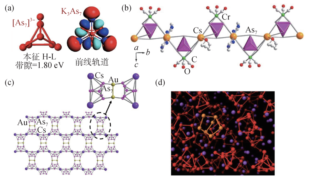
[AS7] 3-cluster has a power gap of 1.8 EV, which can be assembled into materials with different structures and rich properties with a variety of metal atoms. In the experiment, the Castleman team found that AS and K form a cluster in the molecular bundle [55, 5657], where the peaks of AS6K3 and AS7K3 mass spectrum indicate that these clusters are stable. Electronic structure analysis shows that the ionization of AS7K3 is 5.07 EV, and the ionization of AS6K3 is only 3.96 EV, so AS7K3 is a more stable super atom (Figure 5 (a)). In addition, [AS7] 3-and [AS11] 3-Super Atomic clusters can be built with alkaline metals into one-dimensional, two-dimensional and three-dimensional three-dimensional structure (Figure 5 (b)-(d)). [AS7] 3-The one-dimensional system assembled by alkaline metal can change the structure to a spiral shape by changing the chemical measurement ratio from linearity to spiral, as shown in Figure 5 (b) [57]. Use [AS7] 3-or [AS11] 3-cluster as the main construction unit, and combinations with CS+and AU atoms can obtain different two-dimensional thin sheet structures (Figure 5 (C)). In the three-dimensional system, by connecting [AS7] 3-clusters to CS+and K+cation, at the same time, LI+and K+ions can be used as charge balance cations, which can achieve richer geometric shapes (Figure 5 (d)). Electronic structure calculations found that such cluster assembly materials can be manifested as semiconductor characteristics, and the gap will be regulated through alkaline metals [56, 58]: K3AS7 band gap is 1.30 EV, and the adjustment (K-Crypt) 1.5 [AS7K1) .5] and (K-Crypt) [AS7K2] (Crypt fingertips) band gaps were 2.58 EV and 1.98 EV [59]; Large, between 1.97-2.08 EV. Internal construction electric fields can also regulate the capable structure of the AS cluster assembly system [56]: In [(AU2) (AS7) 2] 4−, because there is no adjacent ion to generate an internal electric field, the electrostatic potential gradually decreases; on the contrary,, on the contrary, it,, on the contrary, In the two -dimensional CS4 [(AU2) (AS7) 2], the CS ion produces a large built -in electric field, which happens to be along the front track. Figure 5 (A) The structure of the zero-dimensional [AS7] 3- and the structure of the cluster of the K3AS7 cluster and its front line (right) [56]; CO) 3CS] 3cs] The assembly structure of 3CS [57]; ] The three -dimensional assembly material [56]
The research team also synthesized a series of materials consisting of [AS7] 3-clusters connected by the ⅡB metal ZN, CD and HG to study the impact of the energy-effective assembly on covalent. [56]. The synthetic assembly system includes [Zn (AS7) 2] 4 −, [CD (AS7) 2] 4 −, [hg2 (AS7) 2] 4− and [Hgasas14] 3− AS7) 2] 4 c, [CD (AS7) 2] 4− and free -alkaline metal atoms connected to a three -dimensional arranger. Through element analysis, energy color scattered X-ray spectrum, and X-ray diffraction, it is found that in the system containing ZN and CD, two [AS7] 3-units are connected by metal ions, and in the system containing HG, two [AS7] 3-Unit is connected by HG-HG or HG-AS diode, and optical measurement is 1.62-2.21 EV [59]. Through the charge transfer between the ligand and the cluster, the band gap of the [AS7] 3-cluster assembly system can be regulated: due to the tiny disturbances of the cluster electronic structure, and the lone pairing electronic orbit of the metal cymbal orbital cluster of the metal cymbal orbital cluster Tightly arranged, [AS7CR (CO3)] 3− The band gap compared with [AS7] 3-slightly changed 0.10 EV.
06
Summary and outlook
With the increasing demand for functional materials in modern society, the discovery of the cluster "super atom" has made the concept of material design no longer limited to the traditional atomic structure. A new opportunity is here. The continuous discovery of various "super atoms" with excellent performance clusters has provided a wealth of alternatives for the assembly design of new functional materials, and the development of atomic manufacturing technology has also made the experimental preparation of cluster assembly materials. Although the research work of clusters is still limited, it has indicated that the cluster assembly of the assembly will have broad application space in many fields such as electronic devices, information storage, catalytic, and photonic devices.
The research of cluster assembly is still in the early stages, and many challenges are also faced: (1) exploring new high -quality "cluster elements" (low cost and easy macro -volume synthesis) to meet the integrity and integrity of the element in the assembly process. The needs of stability; (2) During the cluster assembly process, the interaction between clusters should not be too strong (to ensure the integrity of the cluster) or too weak (to ensure the strength and stability of the assembly structure), so clarify the group to clarify the group The law of interaction between clusters and clusters, clusters, and environment is an important issue facing the future; (3) develop new experimental methods to improve the synthesis efficiency of assembly materials, and then accurately prepare cluster assembly materials with specific functions. The huge challenges faced in the experiment; (4) The newly assembled material inquiry is the driving force for further activation and promoting the development of the field. Especially the enlightenment effect of the gathered cluster together will be the future cluster assembly materials. Important topics. Compared with atomic materials, cluster assembly materials not only have rich optionality in the base, but also have the advantages of multi -level structural regulation in terms of material nature. According to the demand orientation, to obtain specific functional materials with the cluster as the base, it is expected to become one of the important ways for the development of new materials in the future. We look forward to not far a long time, scientists can truly realize the leapfrog development of the research of cluster assembly materials from theoretical and experiments, and use cluster "super atom" to construct a new world of material.
references
[1] Bergeron d E, Castleman JR A W, Morisato T et al. Science, 2004, 304: 84
[2] Bergeron d E, Roach P J, Castleman JR A W et al. Science, 2005, 307: 231
[3] Reveles J U, Khanna S, Roach p et al. Proc. Natl. Acad. SCI., 2006, 103: 18405
[4] Castleman JR A W, Khanna S N. J. Phys. Chem. C, 2009, 113: 2664
[5] zhao j, du Q, zhou s et al. Chem. Rev., 2020, 120: 9021
[6] Jena P, Sun Q. CHEM. Rev., 2018, 118: 5755
[7] Rao C n
[8] Weaver J. J. Phys. Chem. Solids, 1992, 53: 1433
[9] Mirkin C A, Caldwell W B. Tetrahedron, 1996, 52: 5113
[10] KRcTSCHMER W, Lamb L D, Fostiropoulos K et al. Nature, 1990, 347: 354
[11] bonifazi d, engine o, diederich f. checkm. Soc. Rev., 2007, 36: 390
[12] Hou L, CUI X, Guan B et al. Nature, 2022, 606: 507
[13] Tsuchiya T, Kumashiro R, Tanigaki K et al. J. am. Chem. Soc., 2008, 130: 450
[14] Li J, Hou S, yao y r et al. Nat. Mater., 2022, https:// doi. Org/10.1038/s41563-022-01309-y
[15] zhang k, Wang C, zhang m et al. NAT. Nanotechnol., 2020, 15: 1019
[16] YAMAMOTO Y, ZHANG G, Jin w et al. PROC. Natl. Acad. Sci., 2009, 106: 21051
[17] zhang x, takeuchi m. Angew. Chem. Int. Ed., 2009, 48: 9646
[18] Guldi d m, GOLOUMIS A, vázquez p et al. J. am. Chem. Soc., 2005, 127: 5811
[19] Segura J L, Martín N, Guldi d m. Chem. Soc. Rev., 2005, 34: 31
[20] Kitagawa S. Chem. Soc. Rev., 2014,43: 5415 [21] TSURUOKA T, Furukawa S, Takashima Y Et Al. Angew. Chem. Int.ed.
[22] Sun D, Tham F S, Reed C A Et Al. ProC. Natl. Acad. SCI., 2002, 99: 5088
[23] Peng p, li f F, neti v s p k et al. Chem. Int. Ed., 2014, 53: 160
[24] KRAFT A, Roth P, Schmidt d et al. Chem.-eur. J., 2016, 22: 5982
[25] KRAFT A, Roger C, Schmidt D et al. Chem. -Eur. J., 2017, 23: 15864
[26] Liang Wenping, Yang Junlin, Chen Yongjun, etc. The physical chemistry of the new century: cutting -edge and outlook for discipline. Beijing: Science Press, 2004
[27] Kumar v. Comput. Mater. SCI., 2006, 35: 375
[28] Kumar V, Singh A K, Kawazoe Y. Phys. Rev. B, 2006, 74: 125411
[29] Guo P, Ren Z y, yang a p et al. J. Phys. Chem. A, 2006, 110: 7453
[30] Khanna S, RAO B, Jena P et al. Chem. Phys. Lett., 2003, 373: 433
[31] Khanna S, Rao B, Jena P. Phys. Rev. Lett., 2002, 89: 016803
[32] Rata I, Shvartsburg a A, Horoi M et al. Phys. Rev. Lett., 2000, 85: 546
[33] Sen P, Mitas L. Phys. Rev. B, 2003, 68: 155404
[34] LIU Z, WANG X, CAI J et al. J. Phys. Chem. C, 2015, 119: 1517
[35] tsunoyama h, Akatsuka H, Shibuta M et al. J. Phys. Chem. C, 2017, 121: 20507
[36] Beck S M. J. CEM. Phys., 1989, 90: 6306
[37] KOYASU K, Akutsu M, Mitsui M et al. J. am. Chem. Soc., 2005, 127: 4998
[38] Nakaya M, iwasa T, TSUNOYAMA H et al. Nanoscale, 2014, 6:14702
[39] LIU J, Guo P, Zheng J et al. J. Phys. Chem. C, 2020, 124: 6861
[40] Shibuta M, Niikura T, Kamoshida T et al. Phys. Chem.phys., 2018, 20: 26273
[41] du Q, Wang Z, zhou s et al. Phys. Rev. Mater., 2021, 5: 066001
[42] zheng Z, Long J R, Holm R. J. am. Chem. Soc., 1997, 119: 2163
[43] Corbett j d. Pure Appl. Chem., 1984, 56: 1527
[44] LEDUC L, Perrin A, Sergent M. Acta Crystallogr. SECT. C-CRYST.STRUCT. Commun., 1983, 39: 1503
[45] zhong x, Lee K, Choi B et al. Nano Lett., 2018, 18:1483
[46] Choi B, Lee K, Voevodin A et al. J. am. Chem. Soc., 2018, 140: 9369 [47] He S, Evans A m, meirzadeh e et al. J. am. Chem. SoC. , 2022, 144: 74
[48] liu Q, zhang Q, shi w et al. Nat. Chem., 2022, 14: 433
[49] Turkiewicz A, Paley D W, Besara T et al. J. am. Chem. Soc., 2014, 136: 15873
[50] Yu j, Lee C H, Bouilly D et al. Nano Lett., 2016, 16:3385
[51] Chauhan V, Reber A C, Khanna S n. Phys. Chem. Chem. PHYS., 2017, 19: 31940
[52] Reber A C, Khanna S n. NPJ Comput. Mater., 2018, 4: 1
[53] ROY X, Lee C H, Crowther a C et al. Science, 2013, 341: 157
[54] li C, Han S, liu Z et al. PHYS. Rev. B, 2022, 105: 115132
[55] Castleman A W, Khanna S N, Sen A et al. Nano Lett., 2007, 7: 2734
[56] MANDAL S, REBER A C, qian m et al. Accounts chem. Res., 2013, 46: 2385
[57] MANDAL S, Qian M, Reber A C et al. J. Phys. Chem. C, 2011, 115: 23704
[58] qian m, reber a c, ugrinov a et al. ACS Nano, 2010, 4: 235
[59] MANDAL S, Reber A C, Qian M et al., 2012, 41: 12365
Reprinted content only represents the author's point of view
Does not represent the position of the Institute of Physics of the Chinese Academy of Sciences
If you need to reprint, please contact the original public account
Source: China Physical Society Journal Network
Edit: Just_iu
- END -
Five time sequence prediction of deep learning model comparison summary: from simulation statistics models to pre -training unsupervised models (attached code)

Source: Deephub IMBAThis article is about 6700 words, it is recommended to read fo...
How annoying is Internet advertisement?Almost the respondents have encountered "unable to close"

Open -columnOn the Internet platform, advertisements are omnipresent. It is a weap...