The total investment exceeds 500 million yuan, and the annual output of Guangchi Semiconductor 120 atomic layers 5 carved erosion machine projects starts
Author:Shanghai Baoshan Time:2022.09.25
Recently, the foundation of the construction of the atomic layer coating and etching equipment project of Guangchi Semiconductor Technology (Shanghai) Co., Ltd. was held. After the project is completed, it will have the capacity of 120 and 5 carved mealing machines with an annual high -precision atomic layer. It will have strong domestic advanced horizontal optical and semiconductor optical field equipment research and development, testing, and service capabilities.
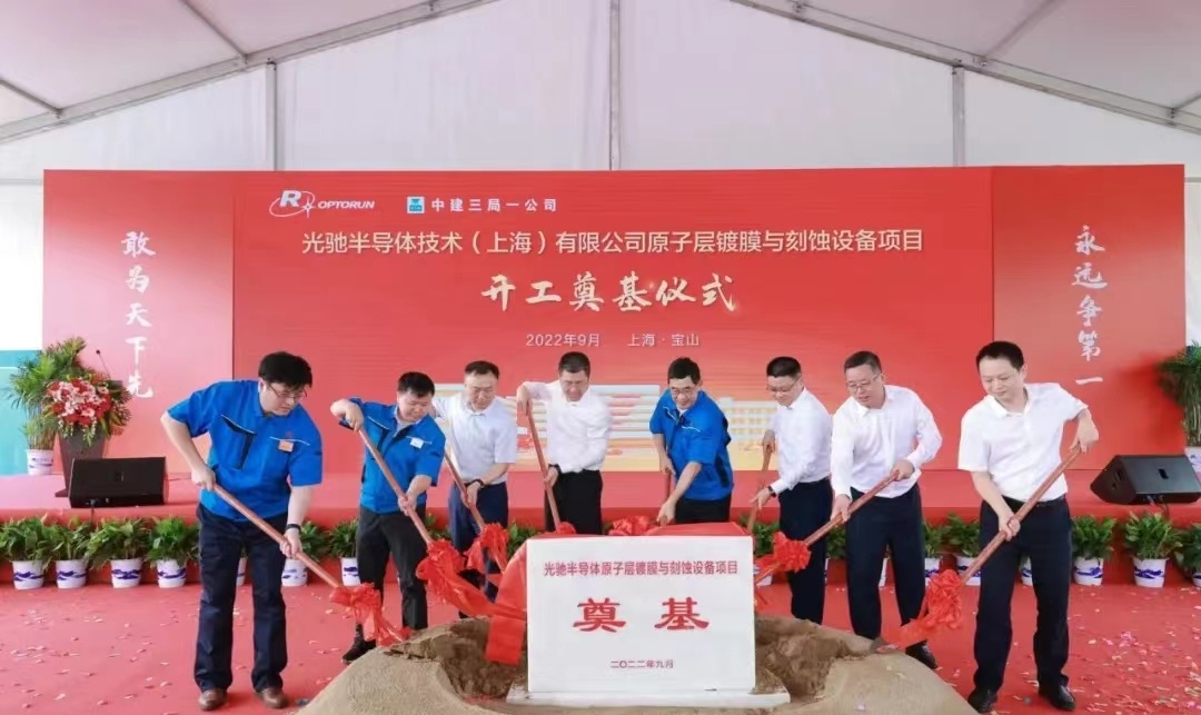
The Guangchi semiconductor project covers an area of 50 acres, with a total planned construction area of about 64,000 square meters, and a total investment of 548 million yuan. The contracting unit is Shanghai Company, a three -bureau of the China Construction Third Bureau of Baoshan High -tech Zone. The project is positioned with new electronic components and equipment manufacturing, and uses the global pan -semiconductor industry chain to adjust with related cutting -edge research and development input and technology integration to achieve industrialization and scale of electronic dedicated equipment manufacturing, and has become an innovation of Guangchi R & D headquarters.
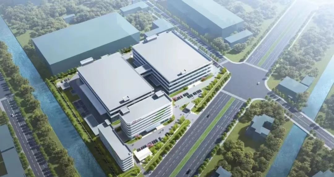
It is understood that the project is planned to achieve annual sales revenue of 365 million yuan after the completion of the first phase of 2024, with a total tax revenue of 23 million yuan in the first phase. The annual property can pay 50 million yuan in taxes to the state, and it is expected to achieve a profit after tax of 210 million yuan. It can effectively promote the north transformation of the Baoshan High -tech Zone, and add bricks to the economic integration of the North and South Parks.
Guangchi Semiconductor Technology (Shanghai) Co., Ltd. is a wholly -owned subsidiary of Guangchi Technology (Shanghai) Co., Ltd., and it is also the first company in the park to invest in land and pick up land in North District. The layout and development of the project in the park is an important part of the improvement of the semiconductor industry in the park. It contributes to my country's solution to related industrial problems in the field of optoelectronics and semiconductor optical fields and achieved large mass production.
Next, the park will continue to make policies+service portfolios, start the brand of Baoshan High -tech Zone, and introduce more high -quality enterprises like Guangchi Semiconductor to the park, take root in the park, so that the smart manufacturing industry such as semiconductors in the park is high standard and efficient to high standards and efficiency. Gathering and development in high quality.
Source: Shanghai Baoshan official WeChat
- END -
@Shenzhen, check today's cute reminder!
After Bai Lu, the weather gradually became coolPhoto ShenzhenWe captured a cute au...
19 provincial and municipal "non -heritage exhibitions" countdown to check in in advance to see the highlights
Video/Snapshot, T_100, F_JPG, M_fast Controls = Controls data-version/ueditor/video/mp4/20220730/1659111238672178.mp4 transcoding = 1 style = width: 400px; Xinjiang is a good place wi